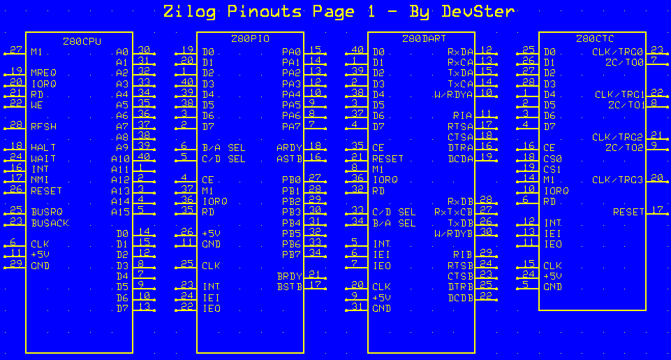
D0-D7: Data bus. Bidirectional, tristate.
PA0-PA7: Port A bus.
PB0-PB7: Port B bus.
ARDY/BRDY: Register A/B ready. If the port is operating in Output Mode, then this signal is active to indicate that the port input register is empty, and is ready for a data transfer to the peripheral device. If the port is in Input Mode, then this signal is active then the port input register is empty, and ready to accept data from the peripheral device. If the port is in Bidirectional Mode, then this signal is active when data is available in the port register for transfer to the peripheral device, and in this mode, data is not places on the port bus unless xSTB is active. Output, active high.
Adress Bus:
A0-A15: Forms the 16-bit address bus. Provides the address lines for memory data bus, or I/O exchanges. All are outputs, active High, and tristate (ON/OFF/HI-Z).
Data Bus:
D0-D7: The 8-bit bidirectional data bus for data exchanged with memory, or I/O. All are input/output, active High, and tristate (ON/OFF/HI-Z).
System Control:
M1: Stands for Machine Cycle 1. When M1 and MREQ are both active, then that indicates that the current machine cycle is the opcode fetch cycle of an instruction execution (first process in getting the opcode/instruction from memory). When M1 and IORQ are both active, then that indicates an interrupt acknowledge cycle (an interrupt response vector can be placed on the data bus). Pin is an output, and active Low.
MREQ: Stands for Memory Request . When MREQ is active, then that indicates that the address bus holds a valid address for reading or writing memory. Pin is an output, active Low, and tristate (ON/OFF/HI-Z).
IORQ: Stangs for Input/Ouput Request. Much like MREQ, when IORQ is active, then that indicates that the address bus (A0-A7) holds a valid address for reading or writing and I/O device. Used for instructions like "IN A,($4F)" or "OUT ($20),A". Pin is an output, active Low, and tristate (ON/OFF/HI-Z).
RD: Stands for Read. Indicates that data is ready to be read from a memory or I/O device to the CPU. Pin is an output, active Low, and tristate (ON/OFF/Hi-Z).
WR: Stands for Write. Indicates that data is going to be written from the CPU data bus to a memory or I/O device. Pin is an output, active Low, and tristate (ON/OFF/HI-Z).
RFSH: Stands for Refresh. Used only for refreshing dynamic memory. The lower 7 bits of the address bus (A0-A6) indicate the refresh address for the memories when MREQ and RFSH are both active. Also used for a good cheap 7 bit counter for output logic :-P. The "R" register can tell us what the lower 7 bits of the address register are going to be. Pin is an output, and is active low.
CPU Control
HALT: Stands for..........."yea duh, we know". Indicates that the CPU has executed a "HALT" instruction. The CPU waits for a maskable, or a non-maskable interrupt before operation can be resumed. Also, during HALT, the CPU executes NOPs to maintain memory refresh for dynamic memories. Pin is an output, and is active Low.
WAIT: When active, the CPU enters a WAIT state. The WAIT pin is generally used for slow ass memory, or I/O devices to indicate that they are not ready for a data exchange. During WAIT state, the CPU does not maintain the memory refresh, so extended WAIT times can make dynamic memories lose data. Pin is an input, and active Low.
Interrupts
INT: Stands for Interrupt Request. An interrupt is generated by I/O devices. An interrupt request is honored at the end of the current instruction if the software-controlled interrupt enable flip-flop (IFF) is enabled. Needs a pull-up resistor. Pin is an input, and active Low.
NMI: Stands for Non-Maskable Interrupt. When triggered, the CPU is forced to restart at location $0066 after the current instruction is executed. NMI has higher priority than INT. The Non-Maskable Interrupt is not affected by IFF. Pin is an input, and negetive-edge triggered.
RESET: Resets the CPU immediatly. It resets the IFF, clears the PC, clears registers I and R, and sets the interrupt status to Mode 0. During the RESET state, the address, data bus, IORQ, MREQ, RD and WR lines are in HI-Z state. RESET must be active for a minimum of 3 clock cycles before the reset operation is complete. Pin is an input, and active Low.
CPU Bus Control
BUSRQ: Stands for Bus Request. Bus request has a higher priority than NMI and is honored at the end of the current machine cycle. BUSRQ forces the CPU address bus, data bus, IORQ, MREQ, RD and WR lines to go HI-Z. When in HI-Z, other devices may control these lines. Extended BUSRQ periods can prevent the CPU from updating memory refreshes. BUSRQ needs a pull-up resistor. Used for DMA operations, dual CPU's, co-processors, etc. Pin is an input, and is active Low.
BUSACK: Stands for Bus Acknowledge. Bus Acknowledge indicates that the CPU address bus, data bus, and control signals have entered their HI-Z states, and that the external circuitry can now control these lines. Pin is an output, and is active Low.
Clock
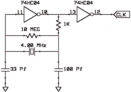
CLK: Square Wave clock input. Example clock using a 4.00 MHz single-phase crystal: